

Key Takeaways
- Input voltage range should set topology choice first, because a source that crosses the target output will push a simple buck or boost stage out of regulation.
- Simulation works best when ideal switching is verified first and losses are added in steps, since that keeps the source of each waveform change visible.
- Parasitics and duty cycle limits carry more weight than clean nominal values, especially in battery-fed systems such as electric vehicle converters.
Buck boost selection starts with the input voltage range, not the converter name.
A lithium-ion cell commonly spans about 3.0 V to 4.2 V during use, which means any pack built from those cells will cross meaningful voltage limits as charge falls. That single fact separates easy converter choices from risky ones. If your source stays fully above or fully below the load target, a simple buck or boost stage will usually fit. If the source crosses the target, a buck boost converter will be the safer model to start with.
That framing matters in simulation because topology errors look acceptable until duty cycle, current ripple, and device stress are checked across the full input range. You are not choosing between three names that do the same job with small differences. You’re choosing the current path that will shape losses, control effort, and usable operating range. Good models make that visible early, before bench work turns a clean schematic into a noisy surprise.
Buck boost fits sources that cross the target voltage
A buck boost converter fits best when your input voltage will move above and below the required output during normal operation. That operating window is the main reason to choose it. It will regulate across the full span where a buck stage or a boost stage alone will lose control at one end.
A battery pack feeding a 48 V bus shows the pattern clearly. Fresh off charge, the pack might sit above 48 V, so a buck stage will work. Near depletion, the same pack can drop below 48 V, so the circuit now needs boost action. A buck boost converter covers both conditions without handing regulation from one stage to another.
This matters because many early models are built around nominal voltage only. That shortcut hides the exact operating points where duty cycle rises, current ripple worsens, and thermal stress starts climbing. If you size the converter around minimum and maximum input first, topology choice becomes much more obvious.
“If you size the converter around minimum and maximum input first, topology choice becomes much more obvious.”
Buck boost action comes from storing energy then releasing it
A buck boost converter works by storing energy in an inductor during one switch state and releasing that energy to the output during another. The control loop adjusts how long each state lasts. That timing lets the stage produce an output above or below the input, depending on circuit form and duty cycle.
A simple inverting buck boost shows the sequence well. When the switch closes, current ramps through the inductor and energy builds in its magnetic field. When the switch opens, the inductor forces current through the diode into the output capacitor and load. The average output level follows the duty ratio, so longer on time raises conversion effect.
You will see the same idea in non-inverting forms used in many power systems. The details differ, but the modelling priority stays the same. Watch inductor current, switch current, and capacitor ripple first. Those waveforms tell you more about converter health than the output voltage alone.
Buck stages cut voltage with simpler current paths
A buck converter lowers voltage with a simpler current path than a buck boost converter, which makes it easier to model and usually easier to control. It fits when the minimum input always stays above the target output. Source current is also more continuous, which often reduces input filtering effort.
A 24 V supply feeding a regulated 12 V controller rail is a clean buck case. The switch applies the input to the inductor for part of each cycle, and the inductor averages that pulsed energy into a lower direct current output. Output ripple is set mainly by switching frequency, inductor value, capacitor size, and parasitic resistance.
You will usually pick buck first when the voltage window allows it because fewer stressed conditions need to be checked. Duty cycle stays in a comfortable middle range more often. That usually means easier compensation, lower peak current, and fewer surprises when the model moves from ideal parts to practical ones.
Boost stages raise voltage through inductor energy transfer
A boost converter raises voltage by charging an inductor from the source and then forcing that stored energy into the load at a higher output potential. It works well when the maximum input always stays below the target output. The tradeoff is that source current and switch stress rise sharply as duty cycle approaches its upper limit.
A 12 V battery feeding a 24 V auxiliary bus is a typical boost case. The inductor charges while the switch is on, and the output capacitor supports the load during that interval. When the switch turns off, the inductor current adds to the source through the diode, which lifts the output above the source voltage.
You should treat high duty cycle results with suspicion, even when the output looks stable. Small errors in switch loss, diode drop, or inductor resistance will distort efficiency quickly. That is why boost models need a close look at current ripple and thermal rise before you accept a neat voltage trace as success.
Simulation should begin with ideal switching then add losses
The best way to simulate a direct current to direct current converter is to start with an ideal switching model, verify waveforms and regulation, and then add non-ideal effects one group at a time. That order keeps faults visible. It also helps you see which parameter actually changes behaviour instead of masking several problems at once.
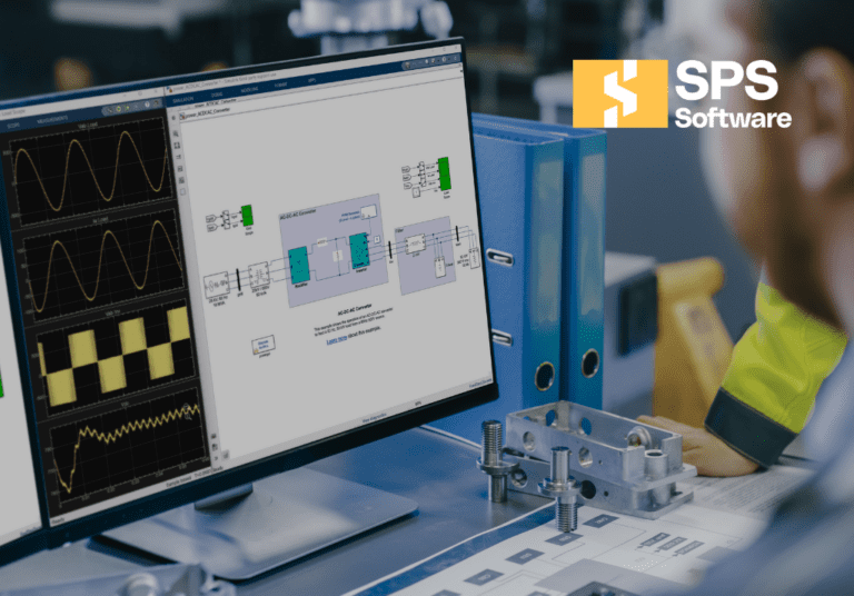
A useful first pass uses an ideal switch, ideal diode, nominal input sweep, and a resistive load. Once duty cycle and waveforms look correct, you add practical loss terms and compare the shift in average output, ripple, and current peaks. SPS SOFTWARE fits this workflow well because the model structure stays open enough for you to inspect each element instead of treating the converter as a sealed block.
- Start with switch timing that gives the expected output across the full input range.
- Add diode drop and switch on resistance before tuning the control loop again.
- Insert inductor winding resistance so current ripple and heating move closer to bench values.
- Include capacitor equivalent series resistance because ripple voltage will rise quickly without it.
- Model dead time and gate delay when switching loss or cross conduction matters.
That sequence will save time because each added loss has a visible signature. If output voltage collapses after resistance is added, the topology or magnetics are likely undersized. If only ripple changes, capacitor choice or frequency will need attention before control tuning starts.
Duty cycle limits explain most topology tradeoffs
Duty cycle limits explain most of the practical difference between buck, boost, and buck-boost choices. When the required duty cycle sits near 0% or 100%, current stress, loss sensitivity, and control margin all worsen. A topology that keeps duty cycle moderate across your operating window will usually produce the cleaner design.
A buck stage is comfortable when input stays well above output, because the required duty ratio stays below unity with margin. A boost stage becomes strained as output rises far above input. A buck boost stage keeps regulation across a wider span, but it pays for that range with more current stress and more parts to tune.
| Use this checkpoint before you commit to a topology. | Read the result as a practical signal from the model. |
|---|---|
| If minimum input stays above target output, a buck stage will usually fit the range. | Duty cycle will stay away from its upper limit, which keeps stress easier to manage. |
| If maximum input stays below target output, a boost stage will usually fit the range. | High load points still need close loss checks because current will climb quickly. |
| If input crosses target output, a buck boost stage will hold regulation across the window. | Current ripple and control effort will rise compared with a single-purpose stage. |
| If the model needs duty cycle near the limits, it is warning you about margin. | Magnetics, switching loss, and transient recovery will become harder to contain. |
Buck boost suits EV batteries that cross the bus
A buck boost converter suits electric vehicle power stages when battery voltage will cross the required bus or subsystem voltage over charge state, temperature, and load. That condition appears often in traction support rails, auxiliary buses, and battery interfacing stages. The topology keeps regulation intact when a buck stage or boost stage alone would fall out of range.
An electric vehicle battery does not sit at one fixed number during use, and that is why this topology matters. Global battery electric car sales reached about 14 million in 2023, equal to roughly 18% of all car sales. A wide and growing installed base means more engineers are modelling battery-fed converters across full operating windows rather than around nominal pack values.
A practical case is a high-voltage pack feeding a lower auxiliary rail during one mode and accepting power from a lower source during another. The exact control scheme will vary, but your model should always sweep minimum pack voltage, maximum pack voltage, and step load conditions. That is where converter choice stops being academic and starts showing its fit.
“Good converter selection comes from that discipline, because the right stage is the one that keeps its behaviour when the ideal parts are gone.”
Parasitics decide if simulated gains survive hardware build
Parasitics decide whether a converter that looks strong in simulation will still behave once copper resistance, capacitor loss, layout inductance, and device timing enter the picture. These effects are not small corrections. They will reshape ripple, peak current, voltage overshoot, and efficiency enough to overturn an early topology choice.
A bench build often exposes this gap at the switching node. The ideal model shows clean transitions, while the hardware shows ringing, extra heating, and output ripple that seemed absent before. That usually traces back to ignored equivalent series resistance, loop inductance, or recovery behaviour. Once those terms are present, the best topology is the one that still meets the target with margin rather than the one that looked best on a clean schematic.
That is the useful habit to keep after the first successful run. SPS SOFTWARE works best when you treat every component as inspectable and editable, then tighten the model until it explains the waveform you expect to measure. Good converter selection comes from that discipline, because the right stage is the one that keeps its behaviour when the ideal parts are gone.