


Key Takeaways
- Accurate power electronics simulation depends more on model scope and validation discipline than on adding extra complexity.
- Device fidelity, parasitics, timing resolution, and steady state setup control most waveform and loss errors in converter studies.
- Reliable results come from checking the model against power balance and independent reference data before accepting plots as truth.
Accurate power electronics simulation starts with model purpose.
Most converter errors come from poor setup choices, not from missing complexity. If you define the study target first, you’ll pick the right model detail, the right time resolution, and the right checks for waveform accuracy, losses, and stability.
“These seven practices address the setup errors that most often distort converter results.”
Power electronics simulation accuracy starts with model purpose
Power electronics simulation becomes trustworthy when the model answers one clear engineering question. That question sets the needed fidelity. It also sets the acceptable run time. You’re far less likely to tune a model around the wrong waveform when the target is explicit.
A ripple estimate for a buck stage needs different detail than a thermal check for an inverter leg. One study cares about switching edges and passive values. The other cares about loss terms and longer operating windows. Keep these scope markers visible before you touch the solver.
- Target waveform
- Operating point
- Needed accuracy
- Time window
- Pass or fail check
These 7 practices improve power electronics simulation accuracy
These seven practices address the setup errors that most often distort converter results. Each one removes a specific source of mismatch between the model and the circuit. Use them in order when you can. That sequence keeps your simulation of power electronics grounded in measurable behaviour.
1. Match device models to the converter operating regime
Device model choice should follow switching speed, voltage stress, thermal range, and the output you need to trust. A simple switch with fixed on resistance works for control tuning in a low-frequency chopper. That same model will miss reverse recovery and output capacitance effects in a hard-switched silicon carbide bridge. You’ll also get the wrong current spike and the wrong loss split during commutation. If your study focuses on average duty response, compact models are enough. If you need turn on loss, diode snap, or dv/dt stress, the device model must include those mechanisms. Model detail should rise only when the study target needs it, or run time will climb without better accuracy.
2. Set parasitic values from measured layout data
Parasitics shape switching waveforms far more than many first-pass models admit. A half bridge with ideal interconnects can look stable and clean, then ring badly on the bench because loop inductance was ignored. A few nanohenries in the commutation path will alter overshoot, current slew, and diode stress. ESR and ESL in the DC link capacitor will also reshape the voltage seen by the devices during edge transitions. You can’t guess these values from textbook schematics and expect good agreement. Pull them from layout estimates, manufacturer data, or measured impedance where possible. Once parasitics are realistic, the simulation stops hiding the resonances that your hardware will actually show.
3. Choose solver steps that resolve every switching event
Time step selection controls whether the solver sees the physics you’re trying to study. A step that skips across turn-on or turn-off intervals will smooth sharp transitions and understate peak stress. A 100 kHz converter with 50 ns edge activity needs much finer resolution than the switching period alone suggests. The same model can look perfectly stable at one step size and clearly unstable at another. Fixed step runs are useful for repeatability, but the step must still capture dead time, diode recovery, and narrow pulses. Variable step runs can help, yet loose tolerances will still bury fast events. If waveforms stop changing when you tighten the step, you’re close to a defendable setting.
4. Start from steady state before capturing waveforms
Waveforms are only meaningful when the converter has settled into the operating point you want to examine. Starting a loss study from zero current and zero capacitor voltage will contaminate the first cycles with startup behaviour. That makes current ripple, switch stress, and average power look worse or better than they really are. A boost converter near 70% duty can need many cycles before the inductor current and output voltage stop drifting. It’s worth running an initial settling window, then collecting data after the transient dies out. You’ll save time during analysis because the measured interval actually represents the target mode. It’s also easier to compare against bench captures taken after the hardware has stabilised.
5. Model gate drive timing with realistic dead time
Gate signals are part of the power stage model because timing errors directly alter conduction paths. Ideal complementary pulses with zero delay can hide shoot-through risk or erase body diode conduction that will appear in hardware. A synchronous buck stage shows this clearly when a few tens of nanoseconds of dead time shift current from the channel into the diode. That shift affects efficiency, reverse recovery, and device temperature. Don’t stop at nominal dead time either. Add propagation delay mismatch, rise and fall differences, and gate resistance effects when those terms matter to the study. If your timing model is too clean, the electrical results will be too clean as well.
6. Check losses with energy balance across each cycle
Loss estimates become more believable when they agree with a simple energy balance. The average input power should line up with output power plus stored energy change plus losses over the sampled interval. If those terms don’t reconcile, the issue is often a sign error, an averaging window that is too short, or missing conduction and switching terms. A phase-shifted full bridge can show plausible switch loss values while total power still fails to balance because magnetics or snubber losses were omitted. Use cycle-based checks before trusting thermal results. It’s a fast way to catch hidden mistakes. Once the power balance closes, every later temperature or efficiency calculation rests on firmer ground.
“Once the power balance closes, every later temperature or efficiency calculation rests on firmer ground.”
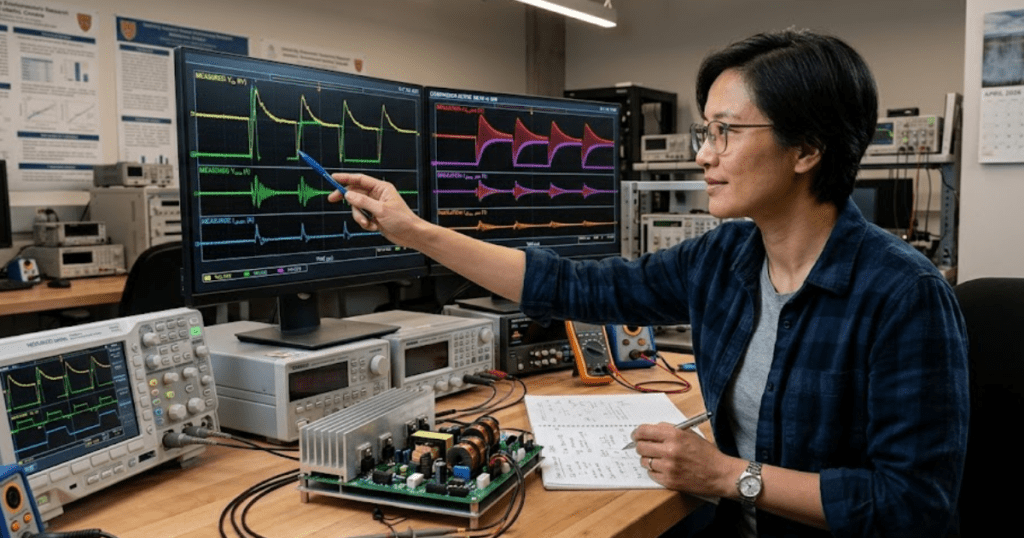
7. Validate waveforms against independent reference results
Validation means comparing the model against something outside the model itself. Bench measurements are strongest, but analytical checks, manufacturer curves, and peer-reviewed reference cases also help. A diode current waveform that matches your expectation in shape but misses the reverse recovery peak still fails validation. The same goes for efficiency results that look smooth yet miss measured conduction loss at light load. Open model inspection matters here because you need to trace what each equation is doing. SPS SOFTWARE fits this step well because the component models are transparent enough for you to inspect parameters, equations, and assumptions instead of treating the block as a sealed box.
| What to focus on | What the practice protects |
|---|---|
| 1. Match device models to the converter operating regime | The chosen device model must include only the switching effects that matter to the study target. |
| 2. Set parasitic values from measured layout data | Measured or estimated interconnect and passive parasitics keep ringing and overshoot from being hidden. |
| 3. Choose solver steps that resolve every switching event | Time resolution must be fine enough to capture narrow pulses and commutation details. |
| 4. Start from steady state before capturing waveforms | Only settled operating intervals should feed ripple, stress, efficiency, and loss checks. |
| 5. Model gate drive timing with realistic dead time | Timing details decide which device conducts and how much switching stress appears. |
| 6. Check losses with energy balance across each cycle | Power balance reveals missing terms and bad averaging before thermal results are trusted. |
| 7. Validate waveforms against independent reference results | Independent checks stop a tidy model from passing when its physics still disagree with measured behaviour. |
How to apply these practices to converter studies

Start each converter study with one operating point, one pass or fail metric, and one validation target. That simple structure keeps the model scoped correctly. It also tells you what detail to keep. You’ll get useful results faster because each setup choice serves a defined purpose.
A classroom buck converter, a lab scale inverter, and a research prototype will all use the same discipline even when their complexity differs. Set the study goal, add only the physics that influence that goal, then verify solver settings, timing, parasitics, and power balance before you trust the plots. SPS SOFTWARE supports this kind of work well because transparent models make each assumption easier to inspect, question, and refine.