

Free Trial
Free Trial
Two engineers inspecting a power converter board under magnifiers
Power Electronics|Power Systems

4 Differences between silicon carbide and silicon MOSFETs in simulation

Key Takeaways

  • Silicon carbide shows its strongest simulation advantage when high voltage and switching loss dominate the converter loss map.
  • Matching gate drive, parasitics, thermal limits, and timing matters more than headline material claims during device comparison.
  • Converter duty cycle ties the main model differences to the final device choice because it sets how often each loss mechanism appears.

Accurate simulation will tell you when a silicon carbide MOSFET earns its place and when a silicon power MOSFET remains the better choice.

Wide bandgap devices can cut power conversion losses by as much as 90% in some applications, which explains why the silicon carbide MOSFET gets so much attention. That headline gain also sets a trap. A simplified model will overstate the benefit, especially when gate resistance, nonlinear capacitance, and junction heating sit outside the study. You need matched conditions before a silicon carbide versus silicon MOSFET result deserves trust.

Silicon carbide fits high-frequency converters with tight loss limits

A silicon carbide MOSFET fits converters where switching loss, bus voltage, and magnetic size set the limit. It performs best in hard-switched or high-frequency stages above a few hundred volts, where silicon devices burn more energy during overlap between voltage and current and during repeated capacitance charging.

An 800 V power factor correction stage running at 100 kHz shows the pattern clearly. Silicon carbide’s critical electric field is roughly 10 times higher than silicon, which allows thinner high-voltage regions and lower resistance in the same voltage class. That material advantage turns into lower simulated loss only when the gate loop and bus inductance reflect the converter you’re actually building.

Frequency alone won’t settle the choice. A 650 V inverter with soft switching can leave less to gain than a 400 V hard-switched boost stage. The useful question is simple: does switching energy dominate your loss map? If it does, a SiC MOSFET will usually repay the extra modelling effort.

Matching test conditions come before any device comparison

Any silicon carbide versus silicon MOSFET study will mislead you unless voltage, current, gate drive, thermal boundary, and parasitics stay matched. Device comparisons fail most often when one model uses default values and the other reflects bench conditions.

“Matching inputs matters more than picking a detailed symbol.”

Lock these five items before you compare parts, or your loss plot won’t mean much.

  • Use the same bus voltage and current waveform for both devices.
  • Set identical gate driver voltage and external gate resistance.
  • Keep loop inductance and stray resistance consistent.
  • Apply the same heat sink and ambient temperature assumptions.
  • Match dead time and the simulation time window.
Checkpoint What stays matched What goes wrong if it drifts
Gate drive conditions Driver voltage, resistance, and source path stay the same for both parts. One switch can look efficient only because it was given an easier turn on or turn off.
Bus parasitics Loop inductance and wiring resistance reflect the same physical layout. Ideal wiring hides overshoot and ringing that fast devices will create on hardware.
Thermal boundary Heat sink, interface resistance, and ambient temperature remain identical. A cooler junction in one model skews conduction loss and safe operating margin.
Load point Bus voltage, current shape, and power level remain fixed during the test. Light-load runs flatter parts that lose ground once current rises.
Dead time Commutation timing stays equal in each leg. Unequal dead time moves diode conduction loss from one device to the other.
Measurement window Both models are averaged over the same settled operating cycles. Short windows can hide heating and capacitance energy that builds over time.

SPS Software helps keep that comparison honest because you can inspect the electrical and thermal assumptions instead of hiding them inside a fixed device block. That matters when a few ohms of gate resistance or a few nanohenries of loop inductance decide the result.

Gate behaviour sets most simulated switching loss results

Gate behaviour decides how fast current rises, how long voltage remains high during turn on and turn off, and how much ringing follows. A silicon carbide MOSFET often looks spectacular in simulation until realistic gate resistance, Miller plateau effects, and source inductance slow the transition.

A 650 V half bridge makes this plain. Set the SiC device with a low gate resistor and an ideal driver, and switching energy falls sharply. Add common source inductance, finite driver current, and separate turn on and turn off resistance, and the advantage narrows to the level you’ll actually see on a board.

The problem isn’t that silicon carbide underperforms. The problem is that gate models are often too kind. Fast edges raise dv/dt, which pushes current through Miller capacitance and can disturb the opposite switch. If you’re modelling a power MOSFET for converter selection, the gate loop is one of the first places to spend effort.

Output capacitance shifts voltage stress during fast edges

Output capacitance shifts voltage stress during fast edges

Output capacitance shapes switching energy, overshoot, and the amount of stored energy that must move during each transition. A silicon carbide MOSFET usually carries lower capacitance at high voltage, but the important detail is its strong nonlinearity. A fixed capacitor value won’t represent that behaviour well enough.

A boost leg at 600 V exposes the issue. Use a constant Coss value from a small-signal table, and the simulated drain voltage slews too smoothly. Use an energy-based or voltage-dependent capacitance model, and you’ll see sharper slope changes, different snubber stress, and a more believable turn off waveform.

That detail matters because capacitance loss repeats every cycle. It also feeds ringing with stray inductance, which affects voltage margin and electromagnetic noise. If your converter uses clamp networks or relies on zero-voltage switching, output capacitance modelling will move the answer more than a tiny change in on-state resistance.

Reverse recovery shapes commutation loss in hard switched legs

Reverse recovery decides how much extra current appears when current transfers from one device path to the other. Silicon carbide parts usually reduce this penalty, while many silicon MOSFETs pay a larger charge extraction cost through the body diode or a companion diode during hard commutation.

A two-level inverter leg gives a clear example. Current freewheels through the lower path during dead time, then the upper switch turns on and must clear stored charge before voltage rises cleanly. If the model omits reverse recovery, the turn-on spike shrinks, the loss estimate falls, and the current stress looks gentler than it will be.

You can’t judge this section from diode charge alone. Dead time, current direction, and junction temperature all shift the result. Hard-switched bridges punish weak commutation behaviour quickly. That is why a silicon device can look fine in a conduction-focused study, then lose ground once you add full transition physics.

Thermal limits decide if efficiency gains survive full load

Thermal limits decide if a simulated efficiency gain survives full load because junction temperature changes resistance, switching energy, and safe operating margin. A cooler device on paper often turns hot once pulse loss, package resistance, and heat sink limits are coupled into the same model.

A 30 kW converter on a shared cold plate shows the risk. At light load, both devices can appear comfortable. Push the model to rated current and include transient thermal impedance, and the hotter switch slows down, loses conduction margin, and can force derating long before the average efficiency number looks alarming.

Steady-state thermal resistance alone won’t protect you here. Cycling duty, startup surges, and uneven leg loading create temperature swings that a single fixed junction value hides. You’re trying to pick a device that stays reliable under stress, so the thermal network must sit inside the switching study, not beside it.

Lower voltage converters still reward strong silicon MOSFET models

Lower-voltage converters often reward strong silicon MOSFET models because conduction loss, package parasitics, and costed gate drive effort outweigh the switching gain of silicon carbide. A SiC MOSFET is not the automatic answer in 48 V, 80 V, or 100 V classes where current is high and voltage is modest.

A 48 V bidirectional converter used for battery buffering is a good test case. The main loss can sit in channel resistance, copper paths, and dead time rather than in high-voltage switching overlap. A modern silicon power MOSFET with low on-resistance and a well-modelled package can outperform a poorly chosen wide bandgap part in total converter loss.

You’re also less likely to need the extreme dv/dt that makes silicon carbide attractive at higher bus voltage. That shifts the design focus toward current sharing, thermal spreading, and package inductance. Good modelling still matters, just for a different reason. You’re checking conduction and thermal balance more than headline switching speed.

Converter duty cycle decides when a SiC MOSFET fits

Duty cycle tells you if a SiC MOSFET deserves the extra modelling burden and device cost. Long high-voltage switching intervals favour silicon carbide. Short low-voltage intervals favour silicon. It turns switching physics into a costed operating pattern you can compare.

“The right power MOSFET choice comes from matched electrical stress, not from material claims or isolated datasheet numbers.”

An 800 V power factor correction stage with frequent hard commutation usually rewards a SiC MOSFET. A 48 V synchronous buck that spends most of its time in conduction usually rewards a strong silicon model instead. Duty cycle links the four decisive simulation differences, because it sets how often gate charge, output capacitance, reverse recovery, and heat actually matter.

SPS SOFTWARE fits this work when you need that judgement to rest on transparent models rather than hopeful assumptions. If you can inspect the gate path, capacitance curves, and thermal network under the same operating point, the silicon carbide choice becomes a measured engineering call instead of a material preference.


Engineer inspecting a power electronics board at a test bench
Modelling

Building high confidence MOSFET models from manufacturer datasheets

Key Takeaways

  • A reliable MOSFET model starts with the converter stress case, not the headline values in the datasheet table.
  • Conduction, charge, and capacitance fitting should be handled in sequence so each parameter set keeps a clear physical role.
  • Trust comes from validation against the original test conditions and from clear limits on where the model has been checked.

A MOSFET model built straight from headline datasheet numbers will miss the losses and waveforms that matter in converter simulation.

Electric motor systems use about 45% of global electricity, which means converter errors don’t stay small once they reach long duty cycles and high power ratings. You need a MOSFET model that reflects the test conditions behind each published curve, not just a few catalogue values. That is the difference between a simulation that only looks plausible and one that supports thermal, efficiency, and control work. High confidence comes from disciplined fitting, not from copying a default MOSFET spice model and hoping the datasheet agrees.

A good workflow starts with the converter stress you need to study, then fits conduction and switching behaviour as separate problems. You’ll get better results when you treat charge and capacitance as voltage-dependent effects and validate against the same tests used in the MOSFET datasheet. That approach gives you a model you can trust inside its calibrated range and question outside it.

Datasheet models fail when test conditions stay hidden

A datasheet curve only describes a MOSFET under the exact bench setup used to measure it. Gate resistance, drain voltage, junction temperature, and stray inductance all shape the published result. Hidden conditions turn copied values into wrong waveforms, even when the MOSFET datasheet looks complete and the model parameters seem reasonable.

A switching plot is a good example. A turn-on time measured at 400 V, 20 A, and 10 Ω gate resistance will not match a converter leg running the same device at 250 V with a 2.2 Ω gate resistor. The curve still has value, but only after you tie it to the stated test circuit. Footnotes, axis labels, and small captions often carry more modelling value than the headline part table.

You’ll also see hidden assumptions around temperature and package parasitics. A transfer curve taken at 25°C can fit threshold behaviour well and still miss current at 125°C. A vendor model that follows one output curve can still fail on turn-off overshoot because the test fixture inductance was never represented. Reading a MOSFET datasheet for simulation means treating every published plot as a conditional result, not a universal truth.

Start with the converter stress that sets accuracy needs

The right MOSFET model starts with the stress case that matters most in your converter. Voltage swing, current level, switching speed, and junction temperature decide which datasheet curves deserve the most fitting effort. A synchronous buck and a hard-switched boost converter will punish different modelling errors.

A 48 V to 12 V synchronous buck usually needs tight low-voltage conduction fitting, because a few milliohms of error will shift efficiency and heat rise at full load. A 400 V boost stage needs stronger charge and capacitance fitting, because switching loss and node overshoot will dominate. Power electronics process more than 70% of the electricity generated in the United States, so model accuracy matters most where converters spend their time and losses.

  • Match bus voltage to the highest and lowest values the device will actually see.
  • Match current to the operating band that sets your thermal limit.
  • Match junction temperature to the condition used for design review.
  • Match gate resistance to the driver network in your schematic.
  • Match switching frequency to the loss mechanism you need to predict.

This priority list keeps the work focused.

“You’re not trying to make a universal MOSFET model on day one.”

You’re trying to build a model that stays faithful where your converter lives. Once that operating window is fixed, parameter choices stop feeling arbitrary and start serving a defined simulation goal.

Separate conduction fitting from switching fitting early

Conduction fitting and switching fitting should be treated as two linked but separate tasks. Channel parameters control current and on-state drop, while charge and capacitance terms control transition timing and energy. Mixing both problems too early makes it hard to see which parameter caused the mismatch.

Start with the steady-state side. Fit the on-state slope and threshold region using output curves, transfer curves, and on-resistance data at the target temperature. A low-voltage server supply gives a clear case, because the simulated drain current at 4.5 V gate drive must line up before you touch rise and fall time. That first pass sets the channel behaviour without the noise of switching parasitics.

Move to switching only after the conduction fit is stable. A common failure shows up when someone stretches gate charge values to force a better turn-on delay, then wonders why the DC current no longer matches the datasheet. You’ll save time if each parameter set has one main job. That separation also makes later validation easier, because each error points to a smaller part of the model.

Use output curves to lock in channel behaviour

Use output curves to lock in channel behaviour

Output curves are the most direct path to a trustworthy channel fit. They show how drain current responds to drain-source voltage across several gate voltages, which lets you set threshold, transconductance, and on-state slope with much less guessing. A good fit here will stabilize every later step.

Pick the gate voltages that overlap your use case instead of fitting every curve with equal weight. A 10 V gate-drive industrial inverter cares far more about the high-current region than the sub-threshold knee. A 4.5 V logic-level design cares about the opposite. The model should match the slope near the operating current, the saturation bend, and the low-voltage resistive region at the same time.

Temperature data matters here too. If the datasheet gives on-resistance against temperature, use it to scale channel conduction after the 25°C fit is complete. That extra step stops the model from looking perfect on one bench plot and failing during thermal sweeps. The checkpoint below helps map the main datasheet plots to the fitting task they should control.

Datasheet plot What it should control in your model
Output characteristics Use these curves to set channel current response across the voltage and gate-drive range you actually switch.
Transfer characteristics Use this plot to refine threshold and transconductance where small gate-voltage errors create large current errors.
On-resistance against temperature Use this relation to keep conduction loss believable during thermal sweeps and hot-load checks.
Gate charge curve Use this plot to shape delay, Miller plateau behaviour, and the timing of voltage and current overlap.
Capacitance against drain voltage Use this relation to model non-linear switching, node ringing sensitivity, and output capacitance energy.
Reverse recovery test Use this test only if the body diode or commutation path matters in your converter leg.

Use charge curves to shape switching behaviour

Gate charge curves are the cleanest way to shape switching behaviour once the channel fit is stable. They capture how the gate current is spent across threshold, Miller plateau, and final enhancement. Rise and fall times only make sense after that charge partition lines up with the datasheet test.

A double-pulse style switching event shows why this matters. If the simulated Miller plateau is too short, drain voltage will collapse too quickly and turn-on loss will look falsely low. If total gate charge is correct but the split between pre-plateau and plateau charge is wrong, the waveform will still miss delay and overlap. You need the model to spend charge in the same order as the device.

Keep the gate loop explicit during this step. The driver voltage, external resistance, and source inductance all shape the current available to charge the gate. A model that matches a datasheet switching plot with the wrong gate network won’t travel well into your converter. This is where many generic MOSFET spice model files look convincing on paper and fail in a half-bridge simulation.

Treat capacitance plots as voltage-dependent functions

MOSFET capacitances are strongly non-linear, so fixed values will distort switching energy and waveform shape. Input, reverse transfer, and output capacitance should follow the drain voltage shown in the datasheet plots. A voltage-dependent fit is required if you want credible turn-off loss, ringing tendency, and dead-time behaviour.

A 400 V switching node makes this obvious. Output capacitance near 20 V can be several times larger than it is near 300 V, so a single Coss value will misstate both stored energy and drain-voltage slew. Reverse transfer capacitance also shifts the Miller effect as Vds changes. That means the same device can look tame in one operating region and much slower in another.

Piecewise fitting is often enough. You don’t need a perfect analytical expression if three or four voltage regions reproduce the plotted capacitance and stored-energy trend. Many engineers also forget the impact on soft-switching intervals and body-diode commutation. Once capacitance is treated as a function instead of a constant, the model starts to carry its weight in converter simulation.

Validate the model against the exact datasheet tests

Validation only means something when the simulation recreates the same test used in the MOSFET datasheet. Match bus voltage, load current, gate resistor, temperature, and reference points before judging the result. That discipline turns curve fitting into model verification instead of a visual comparison exercise.

A useful workflow is to rebuild the published switching or output-characteristic test bench first, then run the device model through the same conditions. If a turn-off plot was measured with a clamped inductive load, the simulation should use the same arrangement and probe points. SPS SOFTWARE fits well here because editable model structure makes it easier to trace a mismatch back to charge, capacitance, or parasitic assumptions instead of hiding it inside a closed block.

“Look for the shape of the error, not only the peak value.”

A correct current peak with the wrong plateau duration means one problem. A correct delay with too much overshoot means another. Validation becomes much faster once each mismatch is linked to a specific physical effect. You’ll also build a record of what the model has already passed, which matters when someone reuses it in another converter study.

Know where the model stops being trustworthy

A high-confidence model is only trustworthy inside the voltage, current, temperature, and gate-drive range used to calibrate it. Outside that range, the same model becomes an estimate. Good engineering practice means marking those limits clearly and refusing to treat one successful fit as universal proof.

A model tuned for a 100 kHz hard-switched leg at 25°C will not automatically predict behaviour in a 20 kHz motor drive at 125°C with a different gate network. The output curves, charge fit, and capacitance fit still provide a strong base, but trust comes from declared bounds. You should write those bounds into the model notes so the next user knows what has been checked and what has not.

That is the standard worth keeping. Converter studies rise or fall on the credibility of the device model inside them, and careful parameter work is what turns a MOSFET datasheet into something useful. SPS SOFTWARE supports that kind of work best when you need open, inspectable models that let you see why a waveform matches, why it misses, and where the model should stop speaking with confidence.

Engineer reviewing subsynchronous resonance waveforms in a grid control room
Power Systems

Capturing subsynchronous resonance in converter-heavy grids

Key Takeaways

  • Subsynchronous resonance is a damping problem that only becomes clear when electrical, mechanical, and control loops are studied as one system.
  • Series compensation and converter controls can both supply energy to a subsynchronous mode, so the source of oscillation must be identified before mitigation is selected.
  • Time domain models with the right control, network, and shaft detail give you evidence you can act on, while steady state studies only tell you where to look next.

Subsynchronous resonance in converter-heavy grids can only be trusted when you study it in detailed time-domain simulation.

Grid composition now includes far more power electronic sources than older screening methods assumed. Renewable capacity additions reached almost 510 GW in 2023, with solar photovoltaic accounting for about 75% of that growth. That shift matters because controls, network resonance, and shaft mechanics can now meet in the same study space. If you rely on steady-state snapshots, you won’t see the feedback loop that turns a mild disturbance into repeated current and torque stress.

Subsynchronous resonance begins with energy exchange below synchronous frequency

Subsynchronous resonance is sustained energy exchange below the grid fundamental, usually between the network and a mechanical shaft or converter control loop. The signal sits under 50 or 60 Hz. Risk appears when damping is low enough for each cycle to feed the next one, so you’re looking for growth rather than a low-frequency component alone.

A practical case helps fix the idea. A 60 Hz system can show an electrical oscillation near 25 Hz after a fault clears on a series compensated line. Current at that frequency can pass through a generator shaft or a wind plant controller and return with more energy than it lost. Oscillography will then show a rising envelope on current, electrical torque, or shaft torque even after the initiating event has ended.

That distinction matters because many studies stop after spotting a resonance frequency. Frequency alone does not confirm a harmful mode. A stable 25 Hz component that decays quickly is a different problem from a 25 Hz mode that grows for several seconds.

“Good studies treat subsynchronous resonance as a closed loop question, with source, path, phase, and damping all represented.”

Series compensation can couple electrical resonance with shaft torque

Series compensation shifts the line’s electrical natural frequency downward, and that can place it close to a torsional mode of a turbine generator shaft. Once those frequencies line up, the network can exchange energy with the shaft every cycle. Torque reversals then rise faster than current plots alone suggest. Torsional interaction becomes visible only when electrical and mechanical states are solved at the same time.

Consider a long transmission corridor with 40% series compensation on a 60 Hz system. The capacitor and line inductance can place electrical resonance near 30 Hz. A nearby steam unit might have a shaft mode around 28 to 32 Hz across turbine sections. A fault, line switch, or power transfer step can then excite both sides at once, and the shaft sees alternating torque that repeats long after voltage appears to recover.

You can miss this with a simplified generator model. A single lumped inertia shows rotor speed movement, yet it won’t reveal which shaft section takes the stress. Utilities learned this in classic SSR events, and the lesson still stands in converter-heavy grids. Series capacitors are not the problem on their own. Trouble starts when compensation, operating point, and a lightly damped mode occupy the same frequency band.

Converter controls can create subsynchronous oscillation in wind plants

Wind plants can produce subsynchronous oscillation when converter controls interact with weak grids, series compensation, or neighbouring control systems. The mechanism sits in software and power electronics rather than a turbine shaft alone. Phase locked loops, current regulators, outer power loops, and dc link controls can all add or remove damping. This is often called subsynchronous control interaction when the controller is the main energy source.

Texas had 42,640 MW of installed wind capacity at the end of 2023. That scale explains why a wind plant connected through a series compensated corridor deserves more than a basic load flow check. One common case uses a doubly fed induction generator plant whose rotor side converter reacts strongly near the network resonance. Another case appears in a full converter plant when a tight phase locked loop meets a weak point of interconnection.

The visible symptom is often current or power oscillation rather than obvious mechanical distress. Plant-level controls can also mask the source because turbines share a collector system and plant controller. If you only check one inverter against an ideal bus, you’ll miss collector impedance, cable capacitance, and controller interactions across units. Converter-heavy grids need plant level modelling before you can trust the damping sign.

Steady state studies miss the feedback loops that matter

Steady state studies miss the feedback loops that matter

Steady state studies miss subsynchronous problems because they solve operating points, not dynamic energy exchange. Load flow, short circuit duty, and basic voltage screening are still useful, yet they can’t show a growing 20 to 40 Hz mode. Control states, limiter action, and phase delay sit outside their scope. You can’t infer damping from a snapshot.

A common failure appears after a voltage dip. The post-fault operating point looks acceptable, line loading is within limits, and capacitor duty seems normal. The converter, though, may pass through a current limit, shift control priority, and return with a different effective impedance at subsynchronous frequency. That sequence decides stability, and it exists only in time.

Protection adds another blind spot. A crowbar, bypass gap, protective relay, or capacitor protection logic can change the network structure during the event you’re studying. Those actions alter frequency, damping, and current path at the exact moment the mode is forming. Screening studies are good for narrowing where to look. They can’t settle if the oscillation will decay, persist, or grow.

Time domain simulation must represent the full feedback loop

Time domain simulation captures subsynchronous resonance only when the full loop is represented from disturbance to response and back again. That means network impedance, controls, protection, and any relevant shaft dynamics must interact at the simulation time step. Event timing matters because milliseconds can alter phase. A model that omits one active part of the loop can give the right frequency and the wrong damping.

A useful study sequence starts with a credible operating point, then applies a specific event such as fault clearing, line energization, or a power reference step. You then track current, electrical torque, shaft torque, control outputs, and bus voltage for several seconds after the event. SPS SOFTWARE fits this workflow when you need transparent models that can be inspected and adjusted instead of treated as sealed blocks. That visibility matters when you’re trying to explain why a mode grows.

Model feature to include What goes wrong if it is omitted Why the omission matters
The series capacitor and its protection states must be modelled. The resonant frequency can shift away from the value seen on the actual line. You will assess the wrong frequency band and miss the event that starts the oscillation.
The shaft must be split into relevant masses when torsional risk exists. A single inertia can hide the section that sees the largest alternating torque. Mechanical stress can be severe even when rotor speed looks modest.
Inner converter loops need their actual gains and filters. Average behaviour can look damped even when the implemented controller adds energy. The sign of damping can reverse with small control changes.
Protection and limiter logic must switch during the event. The study will keep the system in a state that never exists in service. Mode growth often starts during temporary logic states rather than steady operation.
Several operating points should be tested across power transfer and grid strength. A stable base case can hide an unstable condition near a dispatch limit. Subsynchronous risk depends strongly on where the plant is operating.

Good execution does not mean excessive detail everywhere. It means the detail matches the active physics of the loop you are testing. If the question is shaft torque, you need shaft detail. If the question is converter control interaction, controller timing and network frequency response deserve priority. That discipline turns simulation into evidence instead of animation.

Model detail determines if subsynchronous control interaction appears

Subsynchronous control interaction appears only if the model preserves the control dynamics that shape subsynchronous impedance. Average blocks with ideal measurements can erase the delay, filtering, and limiter behaviour that create the instability. The same is true for overly simple network equivalents. Model detail is not about making everything large. It is about keeping the details that set phase and damping at the frequencies of concern.

A grid equivalent behind the point of interconnection can be useful for screening, yet it becomes risky when it hides resonant poles from adjacent lines or collector feeders. A phase locked loop model without its measurement filter can look calmer than the implemented controller. A one mass turbine model can also suppress torsional splitting that matters when electrical resonance sits between shaft modes. Each simplification removes a possible feedback path.

You don’t need transistor-level switching for every study, and you don’t need to model every wind turbine in full detail. You do need the implemented control structure, realistic delays, collector system impedance, and enough mechanical resolution to expose the stress path. If your results swing from stable to unstable after small parameter corrections, that doesn’t mean the simulation failed. It means the system is sensitive and your margin is thin.

Detection depends on mode growth across current, speed and torque

Detecting subsynchronous resonance means checking how a mode grows across electrical and mechanical signals after a credible disturbance. No single trace is enough. Current can look modest while shaft torque rises sharply, and plant power can oscillate while individual controls saturate. You’ll get a trustworthy answer only when signals are reviewed as one coupled response.

  • Track line current spectra below the fundamental after each disturbance.
  • Measure shaft torque or equivalent mechanical stress where rotating machines are present.
  • Record converter internal states such as phase angle, current references, and limiter status.
  • Compare damping at several operating points instead of one dispatch level.
  • Check if the oscillation survives after the initiating event is fully cleared.

A useful diagnostic pattern is rising subsynchronous current, a lagged change in control output, and a matching increase in torque ripple or power oscillation. Another pattern shows stable current at one dispatch point and unstable growth at a higher transfer level, which tells you operating range matters as much as topology. You’ll also want to separate forced response from natural mode growth. A forced oscillation follows an external source, while subsynchronous resonance keeps feeding itself after the trigger ends.

“You can’t manage this class of risk with static studies and broad assumptions, because the damaging mechanism sits in timing, coupling, and damping.”

Mitigation must target the loop that sustains oscillation

Mitigation works when it targets the specific loop that supplies energy to the subsynchronous mode. That could mean shifting the electrical resonance, adding damping in a controller, blocking an operating range, or changing protection timing. Generic fixes waste time because the visible symptom is often far from the actual source. A torque problem can start in a converter loop, and a current problem can start in network compensation.

A line study might show that reducing series compensation moves the electrical resonance away from a shaft mode and ends torsional stress. A wind plant study can show that retuning a phase-locked loop or current controller adds enough damping to stop a 25 Hz oscillation without changing dispatch. Another case can require a supplemental damping function because the plant must keep its compensation level and operating range. Each fix follows from the loop identified in simulation, not from a standard checklist.

Disciplined modelling is what turns subsynchronous resonance from a surprise into a tractable engineering problem. SPS SOFTWARE belongs in that process when you need editable time domain models that show how the loop behaves before equipment absorbs the lesson. That judgment holds across utility studies, research work, and teaching labs because the physics do not simplify themselves for convenience.

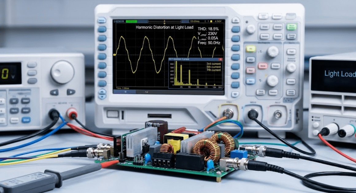
Engineer testing a power converter with an oscilloscope on a lab bench
Power Electronics|Power Systems

Choosing power electronics simulation software for converter design

Key Takeaways

  • The best power electronics simulation software fits the study question and supports the level of detail that question requires.
  • Open device and control models give you results that can be reviewed, adjusted, and defended during design reviews and lab preparation.
  • Speed helps only after model fidelity, workflow fit, and validation checks are aligned with the converter behaviour you need to predict.

Choosing power electronics simulation software for converter design starts with one rule: trust only the models you can inspect and adjust.

More converters now sit inside vehicles, chargers, storage systems, and industrial drives, so small modelling errors carry farther into schedules, test plans, and hardware changes. Global electric car sales passed 17 million in 2024, up more than 25% from 2023. That growth puts more pressure on teams to choose power electronics simulation software that answers the right engineering question instead of producing quick but sealed results.

Converter software choice starts with the study question

The right circuit simulation software depends on the question you need answered. A converter sizing study needs different evidence than a gate timing study. A loss estimate needs different detail than a fault study. Software choice should follow that question first.

A power factor correction stage shows this clearly. If you need input current shape and bulk capacitor size, an averaged model can get you there quickly. If you need switch stress during line transients, the same model will hide the event you care about. A team that skips this distinction usually ends up rerunning work after the first lab mismatch.

You’ll save time when you name the study output before you open the tool. That output might be current ripple, control stability margin, semiconductor loss, or bus overvoltage during a load step. Once that target is explicit, you can judge model detail, solver settings, and result checks with much less guesswork. That is the first filter for any power electronics design tool.

Match model fidelity to the converter behaviour under study

Model fidelity should match the behaviour you need to predict with confidence. Too little detail hides switching effects and parasitics. Too much detail slows routine work without adding useful evidence. Good power electronics design uses the simplest model that still captures the behaviour under test.

A buck converter for control tuning can often start with ideal switches and lumped passive values. The same converter for loss breakdown needs conduction drops, switching energy, dead time, and magnetic resistance. A resonant converter usually needs even more care because waveform shape matters to both efficiency and stress. Fidelity is not a badge of seriousness. It is a fit between the model and the question.

Study focus What the software must represent faithfully
Input and output sizing checks An averaged model is often enough when you only need ripple trends, bus sizing, and steady operating points.
Closed loop tuning The tool should preserve control delays, sampling, and plant dynamics so gain and phase changes appear in the right places.
Switch stress review Switching transitions, parasitics, and commutation paths must be visible or peak voltage and current will be understated.
Efficiency and thermal estimates Device loss mechanisms, magnetic losses, and operating point dependence must be editable or the estimate will look tidy but stay weak.
Protection and fault checks The solver and model set must capture short events, saturation, and controller limits so fault response is not softened away.

Software that supports more than one fidelity level is often the most useful option. You can begin with a fast system model, then move selected sections into switching detail when a question becomes sharper. That staged approach keeps work focused and makes later disagreements easier to trace. It also helps teams compare assumptions instead of arguing over screenshots.

Open device models determine how much results can be trusted

Open device models matter because converter results depend on assumptions that must be visible. If you can’t inspect equations, parasitics, and loss terms, you can’t judge why a waveform looks stable or why a thermal estimate looks low.

“A trustworthy result rests on reviewable model structure and visible assumptions, because polished graphics cannot explain the model.”

A half bridge built with silicon carbide devices makes the point quickly. Output capacitance, reverse recovery, package inductance, and gate resistance all shape overshoot and loss. If those terms sit inside a sealed block, you’re left guessing which default values produced the curve on screen. Editable device models let you test datasheet corners, compare layout assumptions, and document why a parameter changed.

This is where many converter teams lose confidence in their own simulation chain. A result that cannot be audited will stall design reviews, because no one can say which assumption owns the error. Open model power electronics simulation gives you a cleaner path. You can inspect what was modelled, change it deliberately, and explain the impact in plain engineering terms.

Control model access matters as much as circuit fidelity

Control model access matters as much as circuit fidelity

Converter software must expose the control model with the same clarity as the power stage. Sampling, limits, delay, quantization, and protection logic shape current and voltage response just as strongly as device physics. A detailed switching network will still mislead you if the controller sits behind hidden defaults.

A grid tied inverter illustrates the risk. The current loop can look stable in a simplified controller block, then oscillate once saturation, phase delay, and measurement filtering are represented properly. Wind and solar supplied 15.6% of United States electricity generation in 2023, so converter control behaviour now affects far more than a single product bench. Access to the control equations matters because grid interaction, fault ride through, and recovery all sit in that logic.

You should be able to trace a bad transient back to a specific controller assumption. That might be an anti windup clamp, a pulse update delay, or a current sensor filter that was copied from older code. When control models stay open, firmware and power teams can review the same cause chain. That shared visibility turns simulation from a presentation tool into a design tool.

Solver speed matters after accuracy fits the design question

Solver speed is useful only after the model captures the effect you need to see.

“Fast runs support iteration. Fast wrong runs only multiply bad assumptions.”

The best software for converter design gives you enough control over timestep, event handling, and model detail to match speed with purpose.

A resonant converter is a common trap here. Large timesteps can smooth away peak current, soft switching loss, or zero crossing timing that decides device stress. Tightening the solver can expose those events, but it also raises runtime. That tradeoff is acceptable when the question is stress or loss. It is wasteful when you only need a broad operating map.

You’ll get better use from a tool that lets you shift between study modes without rebuilding everything. Start with the plant at a coarse level for operating range checks. Move only the sensitive branch into switching detail when a spike or timing issue appears. Teams often blame the software for slowness when the bigger issue is that they asked one model to answer every question.

Workflow fit depends on integration with control design tools

Workflow fit matters because converter design is rarely a single screen task. You need the circuit model, the controller logic, the parameter set, and the verification notes to stay aligned across revisions. Software that fits your existing control design flow reduces rework and makes reviews far easier.

A digital power supply project shows the difference. The power stage engineer adjusts magnetics and switch timing while the controls engineer tunes current loop gains and fault thresholds. If those edits live in separate files with manual copy steps, mismatches appear quickly. SPS SOFTWARE suits this work when teams need switching level studies with component models they can still open, review, and adapt as assumptions shift.

You should also look at how a tool handles reuse. A good workflow lets you carry a validated leg, filter, or controller into the next design without hiding the equations that made it valid. That matters in industry and in academic labs. Students, researchers, and senior engineers all need the same thing here: a model chain that stays readable after the original author steps away.

Validation methods should reveal assumptions before hardware testing

Validation should expose assumptions early enough to fix them before the first hardware session. Good converter simulation does not end with a plausible waveform. It earns trust through cross checks that tie model behaviour to calculations, datasheets, and measured circuit limits. That is how you separate useful confidence from false comfort.

A practical sequence starts with hand calculations for duty ratio, ripple, and device stress at one operating point. A simplified simulation should match those trends before you add switching details. After that, a detailed model should explain what changed and why, such as diode recovery current or capacitor ESR heating. When the detailed model shifts a result without a clear reason, the issue is usually a hidden assumption or a poor parameter source.

  • The operating point matches a hand calculation at one anchor condition.
  • The control loop still behaves after limits and delays are turned on.
  • The device losses respond sensibly to frequency and current changes.
  • The parasitic values can be traced to layout, package, or datasheet evidence.
  • The model explains any gap between averaged and switching level results.

These checks don’t take long, and they keep lab time focused. You’re not trying to prove a model is perfect. You’re checking that each important assumption is visible, testable, and tied to a physical reason. That discipline is what makes circuit simulation software useful for converters instead of merely convenient.

Common software choices create false confidence in converter results

False confidence usually comes from software choices that hide assumptions behind speed, defaults, or convenience. A clean waveform is easy to trust when deadlines are tight. That trust breaks the moment hardware shows a different switching edge, a slower recovery, or a controller limit you never saw in simulation.

Several patterns show up again and again. Teams pick a tool for its device library, then find that the supplied models cannot be edited enough for a new package or layout. Others run only averaged models, then act surprised when dead time, reverse recovery, or current sampling creates a bench issue. Another group builds detailed switching models but leaves controller delay and saturation at ideal settings, which produces a tidy answer that no firmware build can match.

The safer judgement is simple. Choose power electronics simulation software that lets you inspect the device and control assumptions, match fidelity to the study question, and validate each step before hardware absorbs the cost. SPS SOFTWARE reflects that style of work because switching level modelling and open component models support review, revision, and shared understanding before speed becomes the only thing left to trust.

1 2 3 4 10 11
Cart Overview