

Key Takeaways
-
-
Simulation should define the double pulse test conditions before hardware is powered.
-
Credible switching loss results depend on explicit modelling of the commutation loop and pulse timing.
-
Bench validation gives better answers when the model already explains the expected waveform behaviour.
-
Running a double pulse test in simulation first will save devices, time, and false starts on the bench.
Switching energy, overshoot, and current slope are easier to trust when you study them before probes, fixtures, and layout noise enter the picture. Electric car sales topped 17 million in 2024, which keeps pressure on converter efficiency and semiconductor loss measurement across design teams. That pressure shows up long before final hardware exists. A clean simulation model lets you test the switching event you want under the gate, bus, and load conditions you plan to ship.
A bench double pulse test still matters, but it works best as confirmation. You get more useful lab time when your current target, dead time, stray inductance, and measurement windows are already sorted. That sequence cuts avoidable failures and gives you better turn-on and turn-off energy estimates from the start. Teams that model first reach hardware with questions narrowed to layout, packaging, and measurement accuracy.
A double pulse test isolates one switching transition
A double pulse test isolates a single switching event under controlled current and voltage. The first pulse builds the current you want. The second pulse forces the device through one turn-on or turn-off transition. That is why the method is standard for switching loss characterization.
A half bridge example makes the point clear. You set a bus voltage, place an inductive load in the current path, and use two gate commands separated by dead time. The first command ramps current to a chosen value such as 100 A. The second command captures the commutation event that matters, instead of burying it inside continuous pulse width modulation.
You end up with waveforms that answer practical questions. You can see how much voltage overshoot appears, how steep the current slope is, and how long the voltage and current overlap lasts. Many teams shorten the name to DPT, and some still say DPT test, but the job stays the same. You are isolating one event so the measured energy means something.
Simulation sets up the test before bench hardware
Double pulse test simulation turns the bench plan into a physics problem you can inspect before anything is powered. You choose the bus voltage, loop inductance, gate resistance, and pulse widths first. That gives you a stable starting point. It also shows where the bench setup will be fragile.
A simple simulation setup often mirrors the later fixture. You place a switching device, its freewheel path, a DC link capacitor, an inductive load, and a gate command sequence. A 650 V device on an 800 V bus with a 200 µH load will show if your pulse widths reach the target current and if dead time avoids overlap.
- A DC source with a local link capacitor sets the bus stiffness.
- A switching device model with output capacitance sets the transition shape.
- An inductive current path sets the current ramp before the second pulse.
- A gate network with pulse timing sets the commutation sequence.
- Parasitic resistance and inductance set overshoot and ringing
This step matters because bench work gets expensive once you start guessing. A pulse that looked harmless on paper can overcharge the current or create false ringing from the setup. Sorting those issues in a model keeps the first hardware session focused. You’re no longer using the bench to figure out the test basics.
The commutation loop model determines waveform credibility
The commutation loop model decides if your simulated waveforms deserve trust. Stray inductance and resistance shape overshoot, ringing, and current slope during the transition. Output capacitance and diode recovery also matter.
“A model that ignores those terms will give tidy waveforms and wrong loss numbers.”
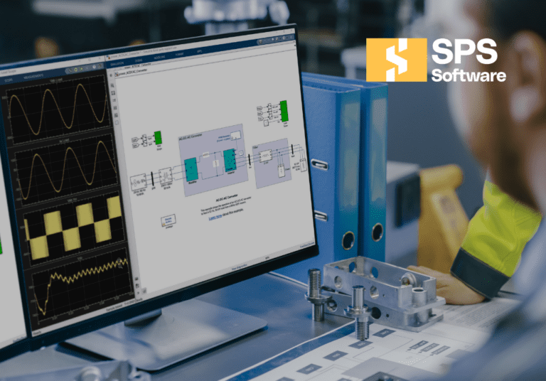
A small numeric example shows why. A loop inductance of 20 nH with a current slope of 2.5 kA/µs produces about 50 V of extra overshoot. SPS SOFTWARE keeps those parasitics visible as explicit model elements, so you can adjust them and see which part of the waveform changes. That’s much more useful than treating the switching leg as a sealed black box.
You don’t need a perfect package extraction to gain value. You need a model detailed enough to reproduce the waveform features that affect energy and stress. Ringing frequency, peak voltage, current tail, and diode recovery spikes are the features worth matching first. Once those are close, the model starts to act like a pre-bench filter for bad assumptions.
The first pulse sets the target current

The first pulse exists to preload the inductor current to a known level before the measured transition. Its width is set from the bus voltage and load inductance. That makes the current target predictable. Good current targeting is what turns the second pulse into a meaningful switching loss test.
A straightforward estimate comes from the current ramp relation. With 400 V across a 200 µH inductance, current rises at about 2 A/µs, so a 50 µs first pulse lands near 100 A if resistive drop is small. That estimate gives you a starting width before you refine the model. You can then trim the pulse until the current sits on the exact test point.
Getting this pulse wrong distorts everything that follows. A current target that is too low will understate turn-on energy. A pulse that is too long will heat the device and shift the result away from the condition you wanted to study. Simulation lets you tighten that first pulse before the hardware ever sees current.
The second pulse captures the switching event
The second pulse creates the transition you care about after current is already flowing. Its timing determines which device turns on or turns off under stress. Dead time sets the starting conduction path. That sequence is what makes the double pulse test useful for switching loss work.
A common case uses the first pulse to build current in the lower device path. Dead time then shifts that current into the opposing diode or body path. When the second pulse commands the lower device on again, you capture turn-on with diode recovery, output capacitance discharge, and loop inductance all present. A different timing choice can instead make the second pulse capture turn-off at the same current level.
You’re not just looking for a clean gate trace. You are checking that the conduction path immediately before the second pulse matches the event you intend to measure. If the wrong path conducts, your waveforms will still look busy, but the extracted energy will describe a different transition. Timing discipline is what keeps the test honest.
Measured waveforms reveal switching stress during the commutation interval
The important double pulse test waveforms are device voltage, device current, and gate signal through the commutation interval. Those traces show where energy is lost and where electrical stress peaks. They also show if the model is missing parasitics. Good interpretation is more valuable than a merely smooth plot.
A rising current spike paired with a delayed voltage fall usually points to diode recovery or extra loop inductance. Several cycles of ringing after the transition often mean your bus loop and output capacitance are badly matched in the model. More than 80% of electricity already passes through power electronics at least once before use, so small waveform errors can scale into poor efficiency estimates across large fleets. That is why waveform reading is more than a lab skill. It is a design filter.
|
Waveform clue |
What it usually means |
|---|---|
|
Voltage overshoot rises right after current falls. |
The commutation loop inductance is too high in the model or in the planned layout. |
|
Current reverses briefly before the voltage settles. |
Dead time or diode recovery is adding extra commutation stress to the event. |
|
Voltage rings for several clear cycles after switching. |
Package capacitance, bus capacitance, or loop damping is missing or scaled badly. |
|
Gate plateau lasts longer than expected. |
Miller charge and gate resistance are stretching the overlap window that creates loss. |
|
Current misses the target before the second pulse starts. |
The first pulse width or the load inductance needs correction before energy is calculated. |
These clues let you correct the model before a single probe is connected. They also tell you what to watch later on the bench. If your simulation shows high overshoot sensitivity to a few nanohenries, you will know layout and probing deserve extra care. That kind of preparation shortens the path from waveform capture to useful engineering judgement.
Separate integrations give each switching energy value
Turn-on energy and turn-off energy come from separate integrations of device voltage times device current over each event. The integration window must cover the overlap interval and stop before later ringing dominates the result. That keeps each energy value tied to one transition. Clean windows matter as much as clean plots.
A practical window starts just before the device voltage begins to move and ends once current and voltage have settled enough that only low-energy ringing remains. A turn-on case might open 20 ns before current rises and close after the main voltage collapse. A turn-off case will use a different window because the current tail and voltage overshoot happen in a different order. You should calculate each event separately rather than averaging first and asking questions later.
This is where simulation earns its keep. You can inspect the time limits, compare energy at several current points, and see how gate resistance shifts the result. If your turn-on loss climbs sharply with a small gate change, you’ve found a sensitive design variable before hardware burns time.
“Bench time works best when it answers a short list of questions instead of defining the whole test from scratch.”
Bench validation starts after the simulation matches expected behaviour
Bench validation should begin only after the simulated double pulse test reproduces the switching behaviour you expect from the device and package. That means current targets, overshoot trends, ringing frequency, and energy windows already make sense. Bench time works best when it answers a short list of questions instead of defining the whole test from scratch.
A disciplined flow is simple. You match the model to the intended topology, adjust parasitics until the waveform shapes look plausible, and then move to hardware with probe placement and current targets already set. SPS SOFTWARE fits that workflow because the switching transition stays transparent enough for you to inspect what each model element is doing. The value is reaching the bench with a test you understand.
That is the judgement worth keeping. Double pulse testing belongs in the lab, but it should not start there. Simulation turns a risky first experiment into a focused confirmation step. You keep more devices intact, spend fewer weeks fixing preventable setup errors, and get turn-on and turn-off numbers with far more context.